Chinese molecular ‘glue’ could pave the way to advanced 3D-printed semiconductors
- ‘3D Pin’ technique helps researchers form stable bonds between suspended nanocrystals to create robust 3D structures
- New materials in the 3D-printing toolbox could mean more cost-effective 3D semiconductors without compromising purity or performance

Three-dimensional (3D) printing has emerged in recent years from a boutique-style manufacturing alternative to become a mainstream conventional manufacturing process in an increasing number of applications across various industries.
The success of a 3D printed project depends largely on the quality of the bonds between the layers or particles in the material, which ultimately affects the properties of the structure.
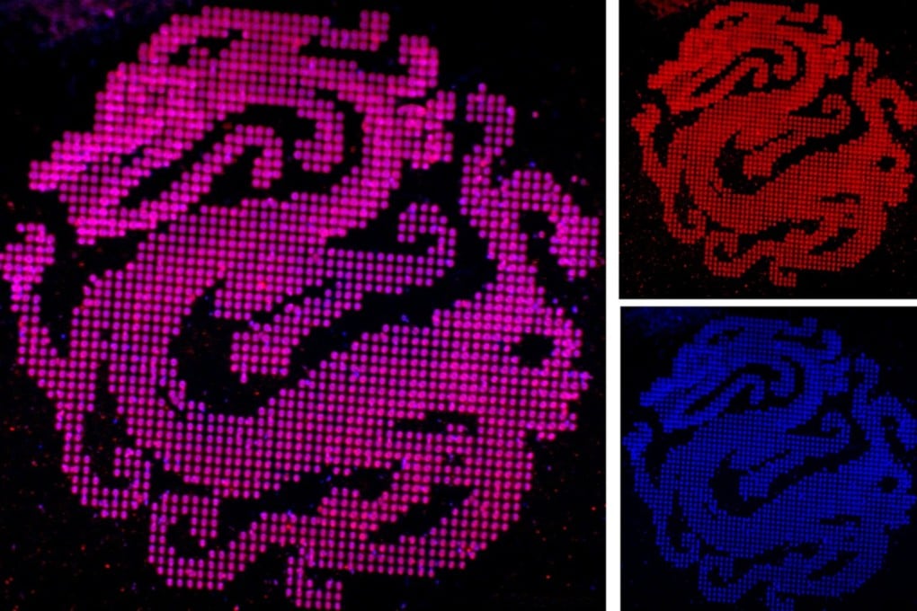
To overcome the obstacle, researchers from Tsinghua University added new materials to the 3D-printing toolbox. The result was the world’s first 3D-printed semiconductor featuring nanometre-level structures.
The work was the first universal approach to 3D-printed semiconductors and other inorganic functional materials with nanoscale resolution, a process that could pave the way for new advances in semiconductor device manufacturing, the researchers said.
The study, co-led by associate professor Zhang Hao, and professors Li Jinghong, Lin Linhan and Sun Hongbo – all from Tsinghua University – was published in the peer-reviewed journal Science on September 28.
The new approach – dubbed “3D Pin” – involved forming semiconductor nanocrystals that were suspended in a specially designed colloidal ink. The team then added a molecular “glue” to the ink that, when laser activated, formed stable bonds between the nanocrystals, resulting in robust 3D structures.